
When AI startup Etched announced its $300 million Series C raise at a $10.3 billion valuation, the tech and AI community took notice. Backed by elite venture backers, including Sequoia Capital, Andreessen Horowitz, Jane Street, Argo, and SK Hynix, the startup presented a bold mandate – to manufacture the application-specific silicon designed to “run the world’s inference.”
Etched also unveiled an 80,000-square-foot, 10-megawatt testing and prototyping facility situated just 15 minutes from its headquarters for managing the surge in transformer compute demands. The decision positions Etched to compete directly with GPU giants like Nvidia by delivering purpose-built, rack-scale inference clusters.
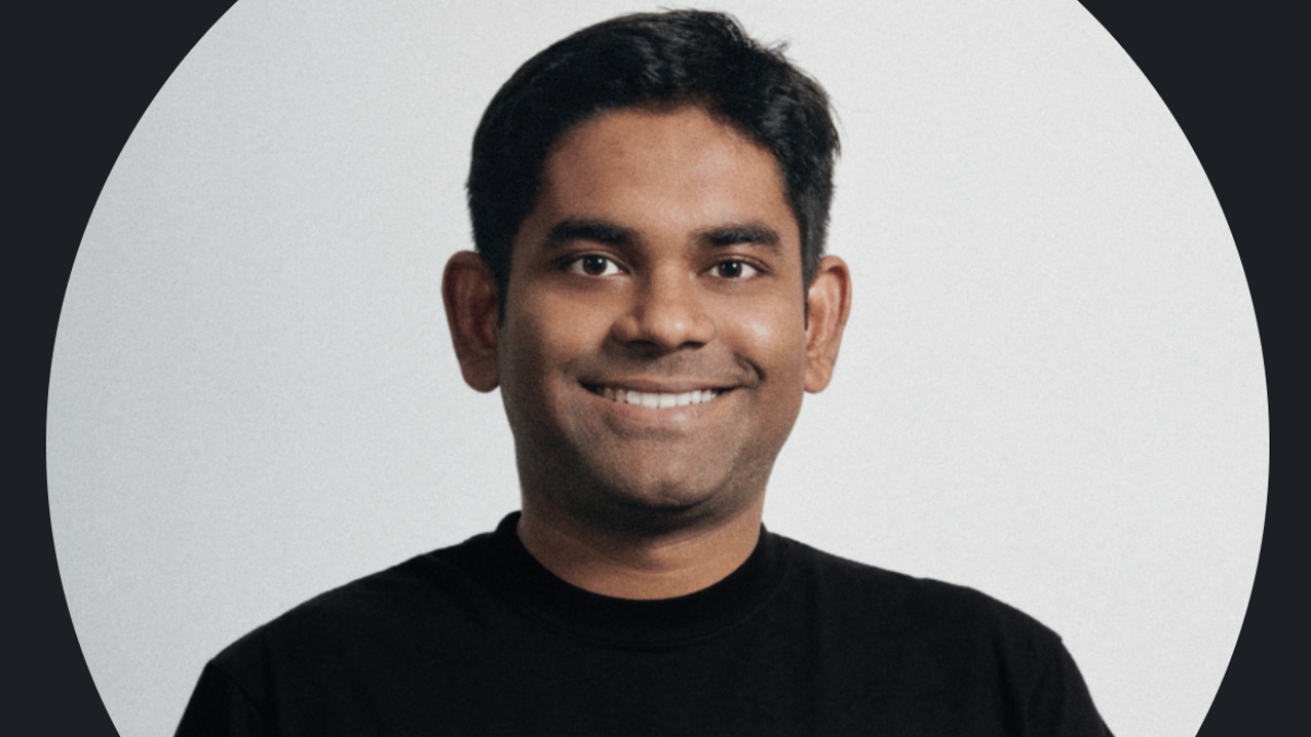
The team behind Etched consists of industry veterans, and chief among them is Dr Saptadeep Pal, the Indian-origin executive who plays a crucial role in the hardware design backing the startup. Pal is the Vice President of ASIC and Architecture, whose chip-design breakthroughs sit at the heart of Etched’s silicon architecture.
Meet Dr Saptadeep Pal: The engineer designing smart chips
Raised in India, Pal’s journey began at the Indian Institute of Technology (IIT) Patna, where he graduated top of his class with an Institute Silver Medal and the Institute Proficiency Prize in Electrical Engineering (B.Tech, ’15).
He then moved to the United States to earn his M.S. (2017) and PhD (2021) in Electrical and Computer Engineering at the University of California, Los Angeles (UCLA). His doctoral research focused on chiplet-based wafer-scale processor architectures – a field that earned him the prestigious Qualcomm Innovation Fellowship in 2019. This also laid the conceptual foundation for next-generation multi-chip systems.
Pal’s role at Etched
As VP of ASIC & Architecture, Pal led the design of Etched’s custom silicon, driving breakthroughs like Low Voltage Inference (LVI), which allows math blocks to run at under half the voltage of standard AI chips to maximise FLOPs density without thermal throttling, enabling maximum FLOPs density while running trillion-parameter Mixture-of-Experts (MoE) models at over 80 per cent peak capacity.
Pal also leads the end-to-end chip architecture for Etched’s specialised ASIC line (including their flagship Sohu chip architectures). Instead of general-purpose compute cores, his designs hardcode the math of transformer neural networks directly into hardware.
With his doctoral background in chiplet-based wafer-scale processors and DRAM stacking, Pal has helped oversee Etched’s proprietary ultra-low-latency interconnects. This hybrid HBM/SRAM memory subsystem eliminates bandwidth bottlenecks between chips, drastically lowering decoding latency for real-time AI workloads.
Pal also works alongside a team of over 400 hardware veterans from NVIDIA, Broadcom, and Google TPUs. He directly connects math block design with inference software, packaging, cold-plate thermals, and manufacturing teams to bring rack-scale systems into production.
Pal’s career milestones
– Early in his career, Pal worked within Nvidia elite architecture research groups, contributing key innovations to the microarchitecture and multi-GPU training strategies underlying the V100, A100, and H100 GPUs.
– Before joining Etched, Pal co-founded Auradine (now Velaura AI), a high-performance infrastructure startup where he spearheaded energy-efficient, low-voltage silicon design and earned multiple foundational patents in clock management and hash engine optimisation.
– Pal holds an expansive list of patents and publications spanning wafer-scale integration, DRAM stacking, low-voltage processing, and fault-tolerant chiplet clocking.