


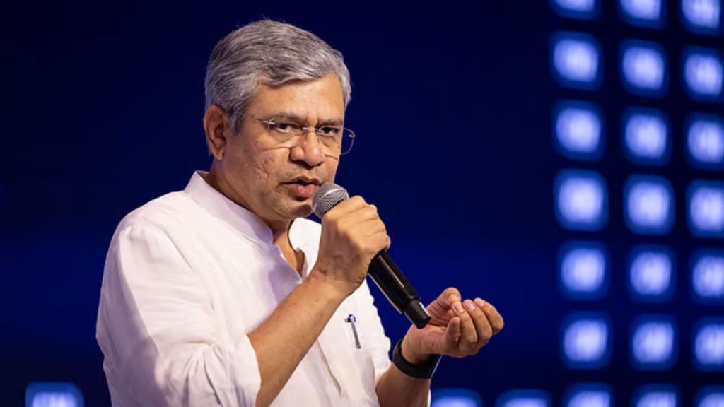

India’s semiconductor push is beginning to move beyond building manufacturing capacity, with India-designed and India-made chips entering products for export to some of the world’s most demanding markets, including Japan, Germany and Switzerland, while the government expects the ecosystem to produce more end-to-end chips in the coming years, Electronics and IT Minister Ashwini Vaishnaw said.
“There would be many made in India and designed in India chips end-to-end,” Vaishnaw told Financial Express Executive Editor-Corporate Rishi Raj during a fireside chat at Semicon India 2026 on Friday. He said assembly, testing, marking and packaging (ATMP) units were already exporting to Japan, while chips were going into products being exported to countries such as Switzerland and Germany. One chip displayed at the event, he said, was also being exported to China.
The developments point to a gradual deepening of India’s semiconductor value chain, from assembly and packaging to chip design, equipment and eventually fabrication. Vaishnaw said indigenisation was taking place sector by sector, piece by piece across the value chain, including semiconductor manufacturing equipment.
He cited the example of Lam Research, which has been able to indigenise an entire complex piece of semiconductor equipment in India, the first time it has done so outside the US. “The biggest strength India has is the design capability,” Vaishnaw said, adding that engineering capabilities built through the IT industry and global capability centres were now moving into electronics and semiconductor manufacturing.
The government is also seeking to build a larger pool of semiconductor talent. Vaishnaw said the focus under Semicon 2.0 would move beyond chip design to system design, after the first phase trained 70,000 design engineers against a 10-year target of 85,000. Around 400 engineering colleges have been given access to industry EDA tools, while chips designed by students are being taped out at the Semiconductor Laboratory in Mohali.
The emphasis on talent is part of a wider effort to establish India as a trusted semiconductor destination. Vaishnaw said global companies were increasingly designing end-to-end semiconductor products in India because they were confident that their intellectual property would be protected.
“India is seen and India is recognised as a trusted country by the world,” he said, adding that this could help the country as semiconductor supply chains become increasingly strategic and geopolitical considerations influence investment decisions.
The semiconductor programme is also becoming closely linked with India’s artificial intelligence ambitions. Vaishnaw said the AI mission, semiconductor mission and electronics manufacturing programmes were interconnected, pointing to the manufacture of complex server components in Pune and interest from global server manufacturers in setting up production in India.
More semiconductor fabs are also expected beyond the Tata Electronics facility being built at Dholera in Gujarat. Asked whether there would be fabs apart from the Dholera project, Vaishnaw said, “Many more. Many more,” without specifying the number or companies involved. The first wafer from the Dholera fab is expected in 2028.
However, Vaishnaw cautioned that the road ahead would not be without risks. He pointed to both internal and external challenges, including the possibility of a disorderly unwinding of accumulated global debt affecting investment flows and the changing geopolitical environment.
“If somebody wants to block India from growing then what are the challenges? How to overcome those challenges?” he said, adding that these were real challenges that India needed to remain cognisant of.
He also acknowledged the complexity of the semiconductor industry and the need for government, industry and academia to work together on faster approvals, upskilling and quality.
Vaishnaw said India was approaching what he described as “escape velocity” in building the semiconductor ecosystem, but stressed that the country still had a long way to go. The next phase, he said, would be about converting the foundation created during the first five years of the programme into a larger ecosystem capable of producing chips, equipment and electronic systems for both the domestic and global markets.