


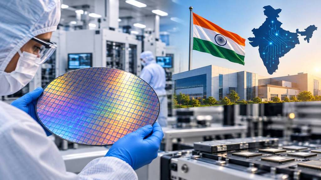

Applied Materials’ $5 billion investment in India by 2035 will help create the supply-chain capabilities, research, talent and required to support the country’s semiconductor ambitions, Chief Operating Officer of Applied Materials India Radhika Viswanathan said.
The US semiconductor equipment maker’s investment will be centred around infrastructure and talent.
“Before we can think through anything, these are the basic foundational steps that we have to do: set up our R&D ecosystem, expand our R&D ecosystem, bring in our ecosystem partners to help set up that R&D ecosystem, extend it into our localised supply chain,” Viswanathan told FE on the sidelines of Semicon India 2026.
A significant portion of the investment will go towards expanding Applied’s R&D footprint and laboratory capabilities in India. The company currently has an active lab space in Bengaluru, alongside cleanroom capabilities for 300-mm wafer processing.
Applied is also looking to develop a proposed 140-acre Advanced Semiconductor Research Park in Bengaluru. The facility will bring together cleanroom infrastructure, equipment engineering and collaborative R&D, while helping build a wider supplier ecosystem.
“We will first expand our own R&D lab strategy. Next, we will expand our ecosystem base, because in this industry you can’t be successful by yourself,” Viswanathan said.
The company plans to expand its supply-chain capacity tenfold by 2035 and grow its network to more than 100 production and R&D suppliers. It will seek to progressively move from sourcing components to building complex modules, sub-systems and eventually full systems in India.
Talent will form the other major leg of the investment. Viswanathan said that while India has significant semiconductor design talent, it currently lacks a large pool of workers trained to run cleanrooms and manage manufacturing processes and equipment inside fabs and foundries.
Applied is working with IITs and other universities to develop specialised coursework. It has launched its Applied Certified Engineer and Applied Certified Technician programmes and plans to more than double its R&D workforce in India by 2035.
“We are not thinking about this as a short-term engagement,” Viswanathan said, adding that the company is assessing what its investment in India needs to look like “over the next decade.”
Applied, which has been present in India for more than two decades, is also looking to use the country increasingly to support its global operations. Demand from artificial intelligence and the development of a domestic semiconductor manufacturing ecosystem are creating opportunities for expansion.
“Where India was five years back versus where we are today, there’s a lot more confidence in terms of putting this investment in place and then leveraging this also to meet the global demand and the scale that is needed,” Viswanathan said.