


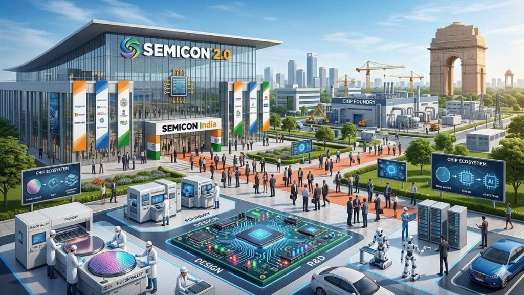

Prime Minister Narendra Modi inaugurated SEMICON India 2026 at Yashobhoomi in New Delhi on Thursday (September 17), placing India’s next phase of semiconductor development in the spotlight. The three-day event, held from September 17 to 19, is expected to showcase how the newly notified Rs 1.27 lakh crore Semicon 2.0 programme will move India beyond chip assembly and expand capabilities across design, fabrication, packaging, equipment, materials and advanced research.
With the theme “Silicon to Systems: Building the Ecosystem,” the fifth edition of SEMICON India will bring together policymakers, global chipmakers, equipment suppliers, investors, researchers, startups and state governments.
The event will also provide the first major industry platform for discussions on Semicon 2.0 implementation, including eligibility conditions, investment thresholds, fiscal support and opportunities for international partnerships.
The central focus of the event will be India’s attempt to build a complete and resilient semiconductor value chain rather than limiting its ambitions to assembly, testing and packaging. The Semicon 2.0 framework covers six broad pillars and 10 categories, including semiconductor design, silicon and specialised fabs, advanced packaging, equipment and component manufacturing, raw materials, research and development, and talent creation.
The programme is designed to support important technologies and strengthen domestic capabilities in areas critical to national security, communications, automotive manufacturing, artificial intelligence (AI), electronics and industrial systems.
The government has notified specific technology, investment, revenue and capacity requirements for companies seeking support under the programme. For silicon wafer fabrication plants, applicants will need to use 300-mm wafers, have a minimum capacity of 40,000 wafer starts per month and deploy production-grade licensed technology.
Such projects must involve at least Rs 20,000 crore in investment and demonstrate minimum revenue of Rs 7,500 crore in at least one of the previous three financial years. Eligible projects will receive government support equivalent to 40 per cent of eligible capital expenditure on a pari-passu basis.
Large global participation
SEMICON India 2026 is expected to be the largest edition of the event so far, with more than 600 exhibitors, including around 300 international companies, spread across 15,000 square metres. The event will feature more than 150 speakers, six country pavilions and 12 state government pavilions.
The exhibition will be organised jointly by the India Semiconductor Mission, MeitY and SEMI, the global industry association for the semiconductor and microelectronics sectors. Companies expected to participate include:
- ASML
- Applied Materials
- Teradyne
- Infineon
- Ebara
- Jabil
- IBM Research
- NXP
- Tata Electronics
- Micron
- Merck KGaA
- Rapidus
- Lam Research
- CG Power
- Uno Minda
- Advantest
- Tokyo Electron
The presence of global equipment makers, chip companies, packaging firms, electronics manufacturers and research organisations will create opportunities for technology partnerships, investment agreements, supplier relationships and manufacturing collaborations.
‘Silicon to Systems’ value-chain showcase
A major attraction will be the “Sand to Silicon to Systems Value Chain Experience,” designed to show how raw materials are transformed into semiconductor wafers, chips, packages and finished electronic systems.
“SEMICON India 2026 will adopt a comprehensive value-chain approach, showcasing the journey from semiconductor materials and manufacturing to advanced packaging, design, electronics and systems,” the Ministry said.Electronics
“The new ‘Sand to Silicon to Systems’ Value Chain Experience will provide visitors with an integrated view of the semiconductor ecosystem and demonstrate India’s expanding capabilities across different stages of the value chain,” it added.
The Startup Pavilion will feature around 40 startups, while the Workforce Development Pavilion will focus on skills, careers and talent requirements in the microelectronics industry. The event will also include student hackathons, keynote addresses, panel discussions, fireside chats and international country roundtables.
The exchange of Memoranda of Understanding marks a significant step towards fostering strategic collaborations and advancing new initiatives across India’s rapidly growing semiconductor ecosystem.
🖇️ Watch Live – https://t.co/3HyPCiCEf2#SEMICONIndia2026 #SEMICONIndia pic.twitter.com/hG5iTQ3I1N
— Ministry of Electronics & IT (@GoI_MeitY) September 16, 2026
PM urges semiconductor CEOs to help build India’s global chip ecosystem
PM Modi on Wednesday chaired a semiconductor roundtable with leading global and Indian industry executives at Seva Teerth, calling for closer government-industry collaboration to shape India’s technology future. Modi urged companies to play a larger role in skilling, innovation and emerging fields such as artificial intelligence and quantum computing.
Referring to India’s target of training one crore people in AI, he said the country’s expanding talent pool, combined with the experience and capabilities of global technology companies, could unlock “significant opportunities.” He also said India should aim to become “among the early leaders” in emerging technologies.
Highlighting the progress made under the India Semiconductor Mission, Narendra Modi said the sector was moving from its foundational phase to “a phase of greater scale and opportunity.” He reiterated the government’s commitment to a predictable and responsive policy environment, while stressing that policies must evolve with technological advances and industry requirements.
The Prime Minister invited industry leaders to submit suggestions on policy and administrative measures and assured them that their views would be considered as India strengthens the semiconductor ecosystem.
CEOs from companies including Micron, Infineon, ASML, Applied Materials, Intel, AMD, Tata Electronics, Foxconn, NXP, Lam Research, Tokyo Electron and IBM Research welcomed the government’s efforts and expressed confidence in ISM 2.0 and India’s potential to build a globally competitive semiconductor hub across manufacturing, R&D, advanced technologies and supporting industries.
Support for specialised fabs and packaging
Semicon 2.0 also provides incentives for segments that require lower investment than large silicon fabs but remain important to the wider electronics ecosystem. Projects involving compound semiconductors, photonics, sensors, microelectromechanical systems and discrete semiconductors will require a minimum investment of Rs 500 crore and revenue of Rs 200 crore. These facilities will be eligible for support of up to 35 per cent of eligible capital expenditure.
Advanced packaging projects, including ATMP and OSAT facilities, will also be supported. Advanced packaging units will require a minimum investment of Rs 1,000 crore and revenue of Rs 200 crore, and will receive up to 35 per cent capital expenditure support. Legacy packaging facilities with similar thresholds will be eligible for support of up to 25 per cent.
As chip designs become more complex, advanced packaging allows multiple chips and components to be integrated into a single high-performance system. This is particularly important for artificial intelligence, data centres, automotive electronics and high-end computing.
New incentives for equipment and materials
One of the key changes under Semicon 2.0 is the government’s effort to support domestic manufacturers of semiconductor equipment, components, raw materials, chemicals and gases. Equipment research and development facilities will need a minimum investment of Rs 300 crore and revenue of Rs 120 crore. Raw-material facilities will require minimum investment of Rs 50 crore and revenue of Rs 20 crore, while test and characterisation facilities will require investment of Rs 100 crore and revenue of Rs 40 crore.
Equipment and component manufacturing facilities will have to meet a minimum investment threshold of Rs 300 crore and revenue of Rs 120 crore. They will be eligible for support of up to 30 per cent of eligible capital expenditure. In addition, a production-linked incentive (PLI) ranging from 10 per cent to 2 per cent will be available for five years from financial year 2028-29, based on the value of components sourced from domestic manufacturers.
The inclusion of these segments is significant because semiconductor manufacturing depends on a large network of specialised suppliers. Domestic fabs cannot operate at scale without reliable access to high-purity chemicals, gases, wafer-related materials, manufacturing equipment and testing systems.
Funding route for chip-design startups
Semicon 2.0 also places substantial emphasis on Indian chip design companies, startups and micro, small and medium enterprises. Eligible startups and MSMEs will be able to receive milestone-linked seed funding equivalent to 50 per cent of project cost, subject to a maximum of Rs 15 crore. Companies backed by venture capital or private equity may also receive equity co-investment, while larger eligible companies may access royalty financing.
Under the royalty-financing model, beneficiaries will pay 5 per cent of the net revenue generated from the supported product or technology until 1.5 times the government assistance has been recovered. For newly launched semiconductor intellectual property, chips and systems-on-chip products, eligible applicants can receive a 9 per cent reimbursement on net sales for five years. The support is capped at Rs 30 crore per application and Rs 120 crore per company, including group companies.
For semiconductor design, companies must be incorporated and headquartered in India, maintain a significant operational and manpower presence in the country, and be owned and controlled by Indian citizens. Commercial semiconductor design companies must also be incorporated and headquartered in India and may be owned and controlled by Indian citizens or Overseas Citizens of India.
Focus on research and sovereign technology
The programme will increase India’s ability to develop and retain important semiconductor technologies. Semicon 2.0 provides government support of up to 75 per cent of project cost for advanced semiconductor research and development, including eligible capital and operating expenditure. The policy is intended to support the development of technologies for critical infrastructure and reduce dependence on overseas suppliers.
The government is also extending electronic design automation tools to academic institutions and startups. According to the Ministry of Electronics and Information Technology (MeitY), the tools have been made available to more than 400 academic institutions and 105 startups, while 24 startups have been approved under the Design Linked Incentive scheme.
From Semicon 1.0 to Semicon 2.0
The event comes as India begins moving from policy creation to project execution under its semiconductor programme. Under Semicon 1.0, the Union government approved 12 semiconductor projects. Three of the approved units have commenced commercial production, according to MeitY. The next phase is intended to build on these projects and address gaps across the supply chain.
Tata Electronics is establishing a chip fabrication plant at Dholera in Gujarat in partnership with Taiwan’s Powerchip Semiconductor Manufacturing Corporation. The project involves an investment of more than Rs 91,000 crore and is planned to have capacity of 50,000 wafer starts per month. The government has committed fiscal support of 50 per cent of eligible project costs under the earlier programme.
Tata Electronics is also setting up a semiconductor facility in Assam with an investment of Rs 27,000 crore. Micron Technology is establishing a semiconductor manufacturing facility in Gujarat with an investment of Rs 22,516 crore.
India’s larger semiconductor ambition
Semiconductors are now viewed as strategic infrastructure because they support almost every major modern industry. Smartphones, vehicles, medical equipment, satellites, payment systems, defence platforms and data centres all depend on chips.
The Covid-19 pandemic exposed the risks created by a concentrated global supply chain. Taiwan remains the dominant producer of advanced chips, while South Korea, Japan, China, the United States and the Netherlands occupy critical positions in manufacturing, equipment, materials and design. India’s strategy is therefore aimed not only at attracting manufacturing investment but also at creating domestic capabilities in design, research, equipment, packaging and systems integration.