


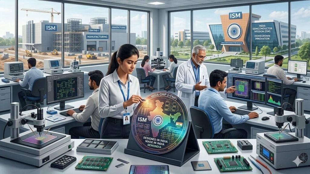

India’s semiconductor programme is moving beyond policy announcements into physical execution, according to a Jefferies report published in September 2026. Construction is under way at sites in Gujarat and Assam, wafers are being processed in clean rooms, and packaged chips have begun emerging from early assembly lines.
Supported by a two-phase incentive framework valued at more than Rs 2 lakh crore, the country has attracted projects from both global and domestic companies across fabrication, advanced packaging, materials, equipment and chip design. The government aims to raise local value addition in electronics manufacturing from the current 18–20% to nearly 35% by 2030 and reduce dependence on imported semiconductors used in automotive, industrial, consumer and defence applications.
Challenges remain in building deeper supply chains, developing specialised talent and competing globally. Even so, the report notes that the focus has shifted from intent to on-ground delivery.
A big policy push behind chips
The Indian government has anchored its semiconductor push within a broader plan to quadruple domestic electronics manufacturing between 2024 and 2031, taking annual production to about $500 billion, according to the Jefferies report. Semiconductors are key to this strategy, helping India move beyond assembly to chip manufacturing,
To encourage this, India has rolled out a Rs 2-trillion semiconductor incentive programme in two phases, alongside existing production-linked incentive (PLI) schemes for electronics and components. The first phase, launched in 2021 with an outlay of Rs 76,000 crore, focused on chip and display fabs, assembly, testing, marking and packaging (ATMP/OSAT) and related facilities.
The second phase, announced in 2026 with an outlay of about Rs 1.28 trillion ($13 billion), widens the net to cover equipment, materials, specialty chemicals and gases, advanced packaging, chip design, R&D and talent development.
Together, these measures aim to create a more complete domestic value chain, where Indian companies can not only assemble devices but also design chips, source critical materials locally and participate in global supply networks.
Phase 1 in action: $20 billion of projects across the value chain
Under the first phase of the semiconductor incentive plan, the government has approved 12 projects with cumulative investments of around $20 billion. These span the entire chain, from front-end fabrication to back-end packaging and specialised materials.
Key projects include:
- A silicon chip fab by Tata Electronics in Gujarat
- An ATMP (memory packaging) plant by Micron
- Multiple OSAT (outsourced assembly and test) facilities by Tata Electronics, CG Power, Kaynes, HCL and Suchi Semicon
- Compound semiconductor fabs by SiCSem and Crystal Matrix
- A glass-substrate packaging project by 3D Glass Solutions
The report added that these initiatives portray India’s first serious foray into front-end fabrication and back-end packaging at scale.
Tata’s $11-billion fab: India’s 1st major silicon foundry
The centrepiece of Phase 1 is Tata Electronics’ $11-billion silicon fab in Gujarat, being set up in collaboration with Taiwan’s PSMC. The plant will produce chips in the 28–110nm node range—mature but critical technologies used in automotive electronics, industrial control, consumer devices and connectivity solutions.
Key features of the project include:
- Designed capacity of around 50,000 wafers per month
- Construction is currently underway, with trial production expected after equipment installation and qualification
- An MoU with ASML for lithography equipment, talent development and supply-chain collaboration
- A strategic alliance with Intel to help build a broader silicon and compute ecosystem in India
- Tata has also signed an MoU with Fujifilm of Japan to develop a local semiconductor materials ecosystem, aiming to reduce dependence on imported chemicals and substrates over time.
- Beyond logic chips, India is moving into display semiconductors as well. Tata Electronics, Taiwan’s Himax Technologies and PSMC have signed an MoU to deliver end-to-end display solutions—from chip design to manufacturing, packaging and electronics manufacturing services (EMS).
Himax, a fabless design leader with about a 40% global share in automotive display driver chips, will collaborate with Tata and PSMC to design and manufacture next-generation display solutions for Indian and global markets.
OSAT boom: Micron, Kaynes, CG Power and Tata’s Assam plant
While fabs attract headlines, the back-end of the semiconductor value chain—where chips are packaged and tested—is already operational and scaling quickly.
Micron (Sanand, Gujarat): Micron’s ATMP facility began commercial production in February 2026, becoming India’s first operational semiconductor ATMP plant under the India Semiconductor Mission. The plant takes DRAM and NAND wafers from Micron’s global network and converts them into finished memory and storage products.
Kaynes Technology (Sanand, Gujarat): Kaynes started production at its $0.4-billion OSAT plant in March 2026, initially focusing on Intelligent Power Modules (IPMs) for automotive and industrial use. Backed by a multi-year supply agreement with Alpha & Omega Semiconductor (AOS) covering 11 package types, the facility is designed to scale to about 6 million units per day at full capacity, with the final phase expected by 2028. Management sees semiconductor packaging revenues ramping up meaningfully from 2028, with revenue visibility of Rs 25,000 crore over the next five years.
CG Power (Sanand, Gujarat): CG Power’s $0.9-billion OSAT facility, set up with Japan’s Renesas Electronics and Thailand’s Stars Microelectronics, commenced commercial production in July 2026. The first shipment went to Renesas customers in Malaysia. CG Power has an off-take agreement with Renesas for about 40–50% of its output. A Phase 2 expansion, due by end-2026, will lift capacity from 0.5 million to 15 million units per day.
Tata Electronics (Assam): Tata’s roughly $3-billion OSAT plant in Assam is under construction, with production expected in 2027. It will package around 48 million chips per day using advanced technologies such as flip-chip and Integrated System-in-Package (ISIP), serving automotive, EV, telecom and consumer electronics. Tata has also partnered with Qualcomm to manufacture automotive modules in India, while L&T Semiconductor Technologies plans to shift backend operations to India and use Tata’s assembly and packaging infrastructure.
Phase 2: $13 billion to deepen the ecosystem
If Phase 1 built the skeleton, Phase 2 is meant to add muscle and depth. The new programme, with an outlay of about Rs 1.28 trillion ($13 billion), is roughly 70% larger than Phase 1 in rupee terms. It broadens incentives across the value chain:
- Up to 40% support for silicon fabs
- Up to 35% for compound semiconductor fabs, display fabs and advanced packaging
- Up to 30% for materials, specialty gases, chemicals and manufacturing equipment
- Up to 75% for semiconductor R&D and talent development
- Crucially, Phase 2 also strengthens domestic chip design through seed funding, equity co-investment, royalty financing and deployment-linked incentives, moving beyond pure capital subsidies. The government expects Phase 2 to attract around Rs 4,00,000 crore ($42 billion) of investment, generate Rs 2,00,000 crore ($21 billion) of semiconductor and electronics production, and drive Rs 1,00,000 crore ($10 billion) of exports.
India bets on mature chip tech to build scale
Analysts note that India is unlikely to match the US or Taiwan at the bleeding edge of chip technology in the near term. Instead, the strategy appears pragmatic: leverage proven, mature technologies that align with domestic demand and economic priorities.
The 28–110nm nodes targeted by Tata’s fab, for example, are in high demand for automotive electronics, industrial control, power management and connectivity—segments where India’s manufacturing base is already expanding.
Now, the focus is on using proven chip technologies to first build reliable and cost-effective production, rather than immediately competing at the most advanced nodes. This can help India build scale, reduce costs and gradually develop capabilities for more advanced chips, according to a Jefferies report.
What are the key challenges?
India’s semiconductor push still faces key challenges, including a limited local supply chain for equipment, materials and components, a shortage of experienced chip-manufacturing talent, intense global competition and rapidly changing technology. While new projects are moving into production and the next phase aims to address gaps in equipment, materials and design, building a competitive chip ecosystem will take time and continued investment.
Rise of indigenous chip design start-ups
India already punches above its weight in chip design. It accounts for roughly 20% of the global semiconductor design workforce and has become a key R&D base for major international players. This talent pool is now feeding a new wave of indigenous start-ups focused on:
- AI accelerators
- Power management chips
- RF (radio frequency) devices
- Automotive semiconductors
- Investor confidence is rising. German chip major Infineon’s recent acquisition of C2i Semiconductors, an Indian start-up working on AI power chips, is seen as a strong vote of confidence in India’s innovation ecosystem.
Government support for design—through seed funding, equity co-investment and deployment-linked incentives under Phase 2—is expected to further encourage this new generation of companies, helping them move from prototypes to commercial products.
India’s semiconductor push is supported by strong fiscal incentives and stable policy support, along with rising demand from electronics, EVs, telecom and defence. Large companies such as Tata, Micron, Kaynes and CG Power are also investing in the sector. Relatively low manufacturing costs, a strong pool of chip-design talent and growing partnerships with Western countries add further support to India’s semiconductor ambitions.