


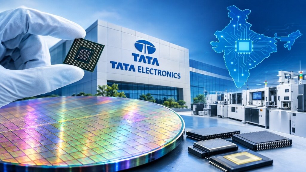

India’s semiconductor push is expanding beyond chip factories to the materials, equipment, suppliers and skilled workers needed to support them. Tata Electronics is building this network around its manufacturing projects through partnerships covering chip production, advanced packaging, design and research.
At Semicon India 2026, the company announced seven Memorandums of Understanding (MoUs) with global technology companies, Indian institutions and infrastructure partners. The agreements aim to strengthen the supply chain for its facilities in Gujarat and Assam, localise critical materials and develop specialised skills.
While MoUs are not immediate revenue-generating contracts, Tata Electronics CEO and Managing Director Dr Randhir Thakur described them as “mutual operational commitments” that lay the groundwork for long-term manufacturing, technology collaboration and ecosystem development.
“These MoUs mean a lot to us. They are measured in terms of the commitment, starting the work, in some cases the development, in other cases providing the infrastructure and getting engaged. So the value part comes much later,” Thakur told media on the sidelines of Semicon India 2026.
Tata Electronics is proud to partner with leading global and Indian organizations across technology, infrastructure, materials, and talent development as we collectively advance India's semiconductor mission.
Day 1 at Semicon India 2026 has been truly memorable, with meaningful… pic.twitter.com/dL9QMdwiX2
— Tata Electronics Pvt Ltd (@TataElectronics) September 17, 2026
- Nexperia: Wafer fab, assembly & test, and tech collaboration
Tata Electronics and Netherlands-based Nexperia have signed a wide-ranging MoU covering:
- Front-end wafer fabrication
- Back-end assembly and test
- Technology and ecosystem development
As part of the front-end collaboration, the two companies are preparing to produce Nexperia’s MOSFET portfolio at Tata’s upcoming 300mm semiconductor fab in Dholera, Gujarat. In parallel, they will collaborate on assembly and test of Nexperia’s discrete semiconductor products at Tata’s packaging facility in Jagiroad, Assam.
Stefan Tilger, interim CEO of Nexperia, said the partnership brings together “complementary strengths across technology, manufacturing and innovation”, while supporting the broader development of semiconductor capabilities in India.
Achim Kempe, COO of Nexperia, added, “This collaboration represents much more than manufacturing… We believe this collaboration creates a strong foundation for future manufacturing, technology development, and ecosystem growth that will ultimately benefit customers around the world.”
- BESI: Advanced packaging capabilities in Assam
Tata Electronics has partnered with BESI, a leading Dutch provider of semiconductor assembly and packaging equipment, to strengthen advanced packaging capabilities at its Jagiroad facility. Under the MoU, Tata will leverage BESI’s portfolio of advanced packaging technologies, including solutions for high-performance computing, AI, data centres, automotive and consumer electronics.
The collaboration will also cover:
- Technical collaboration on next-generation packaging
- Equipment readiness and roadmap planning
- Engineering capability development and specialised training for Tata employees
Dr Randhir Thakur said, “Advanced packaging is rapidly becoming one of the most critical differentiators in semiconductor innovation. By combining BESI’s world-class expertise with Tata Electronics’ growing manufacturing platform, we aim to accelerate the development of advanced packaging capabilities in India.”
The partnership aligns with India’s goal of building a self-sufficient and globally competitive OSAT (Outsourced Semiconductor Assembly and Test) industry.
- SCL: Design, process tech, supply-chain localisation and talent
In a government–private tie-up, Tata Electronics has signed an MoU with the Semi-Conductor Laboratory (SCL), India’s only Integrated Device Manufacturing (IDM) facility under MeitY.
The collaboration will explore joint work in:
- Chip design services for government and startup projects
- Technology node enablement to broaden access to advanced nodes
- Supply-chain localisation for a more resilient domestic ecosystem
- Workforce skilling to build India’s semiconductor talent pipeline
Dr Kanwaljeet Singh, Director General of SCL, said the partnership “amplifies” SCL’s impact by blending its proven end-to-end semiconductor capabilities with Tata’s foundry, OSAT infrastructure and global customer reach.
“Together, we will broaden India’s access to advanced technology nodes, fortify a resilient domestic supply chain ecosystem, and cultivate the next generation of semiconductor talent to secure the nation’s technological future,” he said.
- Fujifilm: Localising critical semiconductor materials
Tata Electronics and Japan’s Fujifilm Corporation have signed an MoU to develop and supply advanced semiconductor materials tailored for Tata’s Dholera fab.
Key elements of the partnership include:
- Localisation of critical raw materials for semiconductor fabrication
- Support to Indian chemical manufacturers with technology, quality assurance and process know-how
- Fujifilm’s planned investment of around Rs 800 crore ($83 million) to set up a semiconductor materials plant in phases at Dholera Special Investment Region (DSIR)
Dr Randhir Thakur said, “Our strategic partnership with Fujifilm marks an important step in strengthening the semiconductor materials supply chain for our Dholera Fab. This will go a long way in building the foundation for a secure semiconductor value chain serving customers in India and around the world.”
Fujifilm President and CEO Teiichi Goto called India’s rapidly expanding semiconductor market a “critical opportunity” and said the partnership would play a “pivotal role” in advancing the country’s semiconductor industry.
- JSR Corporation: Photoresists and advanced chemicals for Dholera
Tata Electronics has also signed an MoU with JSR Corporation for the supply of photoresists and advanced chemicals for its Dholera fab. Photoresists are among the most critical and technology-intensive materials in chip manufacturing, especially at advanced nodes.
Securing a stable supply from a global leader like JSR can be considered as an important step in de-risking the Dholera fab’s material supply chain and ensuring yield stability as production ramps up.
- Ascendas First Space: 363-acre vendor park in Dholera
To accelerate the development of a local supplier ecosystem around the Dholera fab, Tata Electronics has partnered with Ascendas First Space to develop a 363-acre vendor park in Dholera, Gujarat.
The vendor park is intended to:
- Host suppliers of equipment, materials and services for the fab
- Reduce logistics lead times and improve supply-chain resilience
- Create a clustered semiconductor manufacturing ecosystem similar to those in Taiwan, South Korea and Singapore
- Gati Shakti Vishwavidyalaya: Talent for fab engineering and infrastructure
Recognising that semiconductor fabs require highly specialised infrastructure and project execution talent, Tata Electronics has signed an MoU with Gati Shakti Vishwavidyalaya (GSV), a central university focused on transport, infrastructure and logistics.
In collaboration with L&T EduTech and Jacobs Solutions, the partnership will focus on:
- Curriculum development for semiconductor facility engineering and infrastructure systems
- Joint certification programmes
- Industry-oriented skilling in project management, logistics and supply chain for fab construction and operations
Dr Randhir Thakur said, “Semiconductor Fabs are among the most sophisticated industrial facilities in the world, requiring niche expertise across engineering, construction, infrastructure systems, project execution, manufacturing and supply chain management. By combining academic excellence with industry insights, we aim to help bridge critical skill gaps.”
Why these deals matter?
Tata Electronics’ seven MoUs map almost the entire semiconductor value chain. They cover wafer fabrication through the Nexperia partnership for MOSFET production at Dholera; advanced packaging capabilities with BESI at Jagiroad; design and process technology collaboration with the Semi-Conductor Laboratory; critical materials supply via agreements with Fujifilm and JSR Corporation; a dedicated supplier ecosystem through the 363-acre vendor park being developed with Ascendas First Space in Dholera; and a talent pipeline built in partnership with Gati Shakti Vishwavidyalaya, along with L&T EduTech and Jacobs Solutions.
For India, the importance of these deals lies not just in the scale of investment — Tata’s Dholera fab alone is an $11 billion project, with a total of $14 billion committed across the Dholera and Jagiroad facilities — but in the deliberate effort to build a resilient, locally anchored and globally integrated semiconductor ecosystem.
As Dr Randhir Thakur put it, these partnerships are about “starting the work” and “providing the infrastructure and getting engaged”. The financial value, he suggested, will follow — once the ecosystem begins to function.
‘MoUs mean a lot to us’: Tata CEO on strategy and execution
Speaking to media, Dr Randhir Thakur emphasised that these MoUs are not just ceremonial but represent “mutual commitment from both sides”.
“Many of the MoUs are from our partners. They are in Europe, Japan, and Malaysia, and Singapore, and they come through as part of our critical ecosystem because our factories will use 400-plus different suppliers from across the globe,” he said.
Thakur added that Tata Electronics is simultaneously scaling operations across eight domestic sites, covering fabs, electronics manufacturing and packaging.
“Right now, there are so many of these projects going on as we are scaling at eight different sites. So that is currently the mission, really focused on execution,” he said.
On global supply-chain disruptions, he noted that impacts so far have been limited to marginal increases in freight costs, with no major bottlenecks affecting core operations.
Semicon 2.0 and India’s full-stack ambition
Union Minister Ashwini Vaishnaw has described the semiconductor industry as “highly complex”, requiring sustained efforts across multiple layers of the value chain.
Under Semicon 2.0, the government’s focus has expanded from chip fabrication to include:
- Design and IP development
- Equipment and materials
- Advanced packaging
- Research and innovation
- Talent and workforce development
- Resilient domestic and global supply chains
SEMICON India 2026, being held at Yashobhoomi in New Delhi until September 19, features more than 600 participating companies, six country pavilions (Japan, South Korea, Malaysia, the Netherlands, Singapore and Sweden), 12 state booths, a startup pavilion and a workforce development pavilion. The event is expected to attract around 50,000 visitors, including representatives from 52 countries.